The AI Megafactory Revolution Transforming Semiconductor Manufacturing Infrastructure
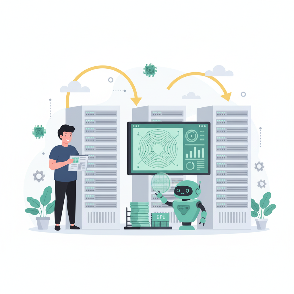
Samsung deploys fifty thousand GPUs at its Taylor, Texas facility to manufacture the advanced chips that power AI systems—including the GPUs themselves. This facility represents more than a semiconductor factory—it’s an example of recursive AI infrastructure, where intelligent systems optimise the production of components that enable more intelligent systems. This self-reinforcing cycle creates compound competitive advantages for early adopters while transforming how semiconductors reach market.
This guide explores Samsung’s AI megafactory through three technical pillars: digital twins enabling real-time yield optimisation, computational lithography achieving twenty times faster optical proximity correction, and HBM4 memory production exemplifying the recursive cycle. You’ll discover competitive dynamics as Samsung challenges TSMC‘s market dominance, the platform ecosystem centred on Nvidia Omniverse, and practical implementation lessons for evaluating AI manufacturing approaches.
Navigate This Guide:
- Digital Twin Manufacturing Optimisation – Technical architecture enabling 30% yield detraction reduction through virtual replicas and predictive maintenance
- Computational Lithography with GANs – How generative adversarial networks achieve twenty times faster optical proximity correction while maintaining quality
- CTO Implementation Guide – Practical frameworks for assessing readiness, evaluating vendors, and designing pilot programs scaled for SMB context
- Competitive Dynamics Analysis – Samsung versus TSMC versus Intel AI capabilities, market share implications, and strategic positioning
- Platform Ecosystem Guide – Nvidia Omniverse, alternative platforms, GPU infrastructure requirements, and integration architecture patterns
Why Are Companies Building AI Megafactories Now?
These facilities represent the convergence of three enabling factors: GPU computing power reaching manufacturing-scale economics, digital twin technology maturing beyond simulation to real-time control, and machine learning algorithms solving previously intractable computational problems like optical proximity correction. Samsung’s 50,000-GPU deployment demonstrates that AI can optimise semiconductor manufacturing with sufficient intensity to create compound competitive advantages—where better AI produces better chips that enable better AI.
The timing stems from reaching inflection points across multiple dimensions simultaneously. Samsung’s deployment at its Taylor, Texas facility represents an industry shift. Rather than deploying AI tools in isolated pockets, the facility operates 50,000 GPUs as cohesive infrastructure powering digital twins of manufacturing equipment, computational lithography optimising photomask designs, and real-time defect detection across production lines. This scale transforms AI from supporting tool to central nervous system.
GPU economics have shifted—Nvidia’s H100 and B200 accelerators deliver performance enabling manufacturing-scale deployment at viable costs. Digital twin technology has matured from offline simulation tools to systems synchronising with physical processes in real time, enabling risk-free testing of optimisations before applying them to production. Computational breakthroughs like Samsung’s twenty times optical proximity correction improvement prove AI can solve problems previously considered computationally impossible.
Advanced manufacturing nodes at 3nm, 2nm, and approaching sub-2nm scales demand precision beyond human-designed processes. Light diffraction at nanometre scales, atomic-level defect detection, and maintaining equipment operating within tolerances measured in angstroms require intelligent systems capable of processing sensor data and adjusting parameters faster than human operators can comprehend, let alone act upon. HBM4 memory requirements create supply bottlenecks that AI-enhanced manufacturing addresses by boosting yields and accelerating production ramps.
Early adoption advantages compound over time. Samsung’s 30% yield detraction reduction translates directly to higher effective capacity without building additional fabrication facilities. Their twenty times OPC improvement accelerates design-to-production cycles, enabling faster customer response and new product introduction. These benefits accumulate as production data trains machine learning models that become progressively more accurate at predicting optimal parameters, creating organisational learning advantages that late adopters cannot easily replicate.
Understanding how Samsung compares to TSMC and Intel in this competitive race reveals why timing matters—early leadership in AI manufacturing may determine who dominates semiconductor production over the coming decade.
What Is the AI Megafactory Concept and How Does It Work?
This approach deploys thousands of GPUs as unified infrastructure integrating digital twins of manufacturing processes, real-time machine learning for defect detection and yield optimisation, and AI-enhanced computational tools like optical proximity correction. Samsung’s Taylor, Texas facility uses 50,000+ Nvidia GPUs to create a single intelligent network where virtual replicas of physical equipment enable predictive maintenance, process optimisation, and quality control at scales impossible with traditional automation.
Samsung’s implementation centres on Nvidia’s Omniverse platform as the foundation for digital twin creation and management. Each piece of manufacturing equipment—lithography systems, etching tools, deposition chambers, inspection stations—has a virtual replica synchronised with its physical counterpart through real-time sensor data. These digital twins enable engineers to test process changes virtually, predicting how adjustments to temperature, pressure, chemical concentrations, or timing parameters will affect yield before touching production equipment.
Manufacturing Execution Systems coordinate production schedules and track wafers through hundreds of process steps. IoT sensor networks provide real-time data on equipment status, environmental conditions, and in-process measurements. The AI infrastructure processes this data continuously, with bidirectional feedback loops—AI insights trigger process adjustments, which generate validation data that improves model accuracy.
Samsung’s Taylor facility showcases this integration at scale. The location represents geographic diversification beyond South Korea, establishing US manufacturing capacity while serving as a technology showcase. The facility targets 2nm GAA transistor production using AI optimisation across the entire manufacturing flow. Partnership with Nvidia provides not just GPUs but the Omniverse platform and manufacturing-specific AI development support.
Timeline milestones demonstrate progress from announcement to production. The 2025 announcement established the vision. Production shipments of HBM4 memory begin in Q2 2026, demonstrating AI manufacturing producing the advanced memory enabling next-generation AI accelerators—closing the recursive loop. By 2027-2028, expansion plans target 50,000-100,000 wafers per month capacity at sub-2nm nodes, representing full-scale operations.
Legacy equipment augmentation versus greenfield deployment represents a choice you’ll face when implementing AI capabilities. Greenfield facilities like Taylor can architect AI integration from foundation, but most manufacturers must retrofit AI capabilities onto existing fabs with equipment representing billions in capital investment. This requires different integration strategies, phased deployment, and careful change management to maintain production continuity.
For evaluating AI manufacturing, understanding the platform ecosystem surrounding Nvidia Omniverse and alternative approaches helps assess viable paths forward.
How Do Digital Twins Enable Real-Time Yield Optimisation?
Digital twins create virtual replicas of manufacturing equipment and processes that synchronise continuously with physical operations, enabling risk-free testing of optimisations, predictive failure detection, and real-time process adjustments. Samsung achieves 30% reduction in yield detraction by using digital twins for predictive maintenance, defect detection through computer vision, and process control where machine learning models predict optimal parameters across temperature, pressure, chemical concentrations, and timing variables.
The digital twin architecture consists of several integrated components. Virtual replicas model physical fab equipment and processes using physics-based simulation combined with data-driven machine learning. Continuous synchronisation mechanisms keep virtual and physical systems aligned through IoT sensor data streams providing real-time measurements. Machine learning models trained on historical production data predict outcomes from process parameters, with twin-physical alignment mechanisms ensuring predictions remain accurate as equipment ages and conditions drift.
Three primary applications deliver quantifiable business value. Yield optimisation uses machine learning models to predict final chip yield from early-stage measurements—electrical tests performed after initial layers can forecast whether a wafer will meet specifications after hundreds of subsequent process steps. This enables intervention before investing additional processing time and materials in wafers unlikely to yield functional chips. Samsung’s 30% reduction in yield detraction represents the percentage of potentially salvageable wafers rescued through AI-recommended process adjustments.
Defect detection applies computer vision at nanometre scale to identify defects faster and more accurately than human or traditional optical inspection. Scanning electron microscopes generate high-resolution images of wafer surfaces. Machine learning models trained on millions of images learn patterns distinguishing defects from harmless variations, reducing false positives that stop production lines unnecessarily while catching subtle anomalies human inspectors miss.
Predictive maintenance analyses sensor data patterns to predict equipment failures before they occur. Vibration sensors, temperature monitors, gas flow measurements, and power consumption data feed into models that recognise signatures of developing problems—bearing wear, heating element degradation, seal leaks, or contamination buildups. Scheduling maintenance during planned downtime prevents unexpected failures that idle expensive fabrication equipment and potentially scrapping in-process wafers.
Quantitative business impact demonstrates ROI. Samsung’s 30% yield detraction reduction translates directly to higher effective capacity—more functional chips from the same silicon input. Predictive maintenance reduces unplanned downtime, improving equipment utilisation rates. Faster production ramp-up through virtual commissioning shortens time from installing new equipment to reaching target yields. Implementation timelines typically target 12-24 months for digital twin deployment, with benefits accelerating as models accumulate training data.
Implementation requires data infrastructure. Real-time streaming architectures handle continuous sensor data flows. Data lakes store historical production data for model training. Processing infrastructure runs inference workloads as wafers progress through manufacturing. Integration with Manufacturing Execution Systems, SCADA systems, and quality management platforms coordinates the intelligent network.
Platform selection involves evaluating Nvidia Omniverse against alternatives like Siemens Digital Twin, Dassault 3DEXPERIENCE, or open-source combinations. Organisational capability requirements span data scientists who develop machine learning models, manufacturing engineers who understand process physics, and integration specialists who connect AI infrastructure with existing systems.
For comprehensive technical architecture, implementation patterns, and how to deploy digital twins in semiconductor manufacturing, the dedicated guide provides detailed blueprints and integration strategies.
How Did AI Achieve Twenty Times Faster Optical Proximity Correction?
Generative adversarial networks reduced optical proximity correction computation time by 20x while maintaining manufacturing quality by learning optimal photomask patterns from training data rather than computing physics simulations. Samsung’s breakthrough applies generator-discriminator networks to predict how light diffracts at nanometre scales, replacing computationally expensive model-based OPC with trained neural networks that generate high-quality masks in fraction of the time, enabling faster design-to-production cycles for advanced nodes.
Optical proximity correction addresses a physics challenge. At 3nm, 2nm, and sub-2nm manufacturing nodes, the wavelength of light used in photolithography exceeds the feature sizes being printed. Light diffracts around edges and corners, causing circuit patterns to transfer imperfectly from photomask to silicon. OPC compensates by pre-distorting mask patterns so diffraction produces the intended result on the wafer.
Traditional model-based OPC solves this through intensive physics simulation. Software models light propagation through the optical system, predicts how patterns will print on silicon, compares results to design intent, then iteratively adjusts the mask design. This computational loop repeats until predicted results meet manufacturing tolerances. For complex patterns at advanced nodes, this process requires hours to days of computing time, creating bottlenecks in chip design cycles and delaying time-to-market.
The GAN architecture for lithography adapts the generator-discriminator framework from image synthesis. The generator network creates optimised photomask patterns from design intent. The discriminator network evaluates whether patterns will produce acceptable results when manufactured, trained on historical data of successful mask designs and their measured outcomes. During training, the generator learns to fool the discriminator by creating masks that pass quality checks, learning the complex non-linear relationship between mask patterns and final results.
Samsung’s implementation demonstrates the approach’s viability. Training on years of production data from successful mask designs gives the GAN models deep pattern libraries encompassing edge cases and corner scenarios. Inference speed delivers the promised 20x improvement—what required hours of simulation now completes in minutes. Quality validation confirms AI-generated masks meet or exceed traditional OPC accuracy, with measured defect rates and yield outcomes matching or improving upon model-based approaches.
Manufacturing enablement at advanced nodes depends on this breakthrough. GAA transistor production at 3nm and 2nm nodes requires precise OPC managing three-dimensional structures and multiple patterning steps. Faster OPC accelerates design iteration cycles—when engineers can test mask variations in minutes rather than hours, they explore more options and converge on optimal designs faster. Time-to-market advantages compound for customers requiring rapid customisation or new product introduction.
The broader implications extend beyond semiconductor manufacturing. The principle of replacing expensive physics simulations with trained neural networks applies wherever computational bottlenecks constrain optimisation. Transfer learning demonstrates that GAN architectures developed for image synthesis adapt to domain-specific optimisation challenges when trained on appropriate data. Validation methodology becomes critical—ensuring AI solutions meet manufacturing quality standards through rigorous testing against known benchmarks.
For evaluating where AI might solve computational bottlenecks in your operations, understanding Samsung’s 20x optical proximity correction breakthrough with its technical architecture, performance benchmarking, and quality validation provides a template for identifying similar opportunities.
What Is HBM4 Memory and Why Does It Matter for AI Infrastructure?
HBM4 represents next-generation High-Bandwidth Memory technology critical for AI accelerators, featuring increased bandwidth and capacity versus HBM3E. Samsung’s Q2 2026 production timeline demonstrates the recursive AI infrastructure cycle: AI-enhanced manufacturing enables HBM4 production, which in turn powers more capable AI accelerators that drive demand for even more advanced manufacturing capabilities—creating self-reinforcing competitive advantages for early adopters.
HBM4 specifications advance beyond current HBM3E memory used in Nvidia H100, H200, and AMD MI300X accelerators. While specific bandwidth and capacity figures await final specification release, the progression from HBM3 (819 GB/s per stack) to HBM3E (1,150+ GB/s) to HBM4 continues the trajectory of doubling bandwidth roughly every 18-24 months. Increased capacity per stack enables larger AI models and more complex simulations. Samsung’s production timeline targeting Q2 2026 shipments positions them alongside SK Hynix in the competitive race for next-generation AI memory supply.
The recursive AI infrastructure cycle becomes tangible through HBM4 production. Stage one deploys AI megafactory capabilities—digital twins optimise production processes, computational lithography accelerates mask design, and predictive maintenance maximises equipment uptime. Stage two applies these capabilities to manufacture HBM4 with higher yields and better performance than traditional manufacturing could achieve. Stage three sees HBM4 integrated into more powerful AI accelerators enabling larger models and faster training. Stage four uses those advanced accelerators to power next-generation manufacturing AI, and the cycle repeats with compound improvements.
Strategic implications span multiple dimensions. Memory bandwidth represents a primary bottleneck for AI accelerators—GPUs can process data far faster than memory can supply it. HBM4 addresses this constraint by increasing the data transfer rate between memory and processing units. Supply chain positioning becomes critical as HBM production capacity constrains AI accelerator manufacturing. Companies with captive HBM production gain supply security and cost advantages. Vertical integration benefits accrue to Samsung, which manufactures both logic chips and memory, enabling optimised co-design and production coordination.
Customer implications ripple through the AI infrastructure ecosystem. Nvidia, AMD, and other AI accelerator manufacturers depend on HBM suppliers for memory components. Data centre operators planning AI infrastructure roadmaps must account for HBM availability timelines. Cloud service providers offering AI training and inference services require visibility into next-generation accelerator specifications and availability. The entire AI technology stack from training frameworks down to data centre power infrastructure scales with accelerator capabilities enabled by memory advances.
Tangible product outcomes exemplify recursive infrastructure. HBM4 represents physical evidence that AI builds the components that build AI. Unlike abstract discussions of AI potential, memory chips shipping to customers in 2026 close the loop concretely. Timeline visibility demonstrates near-term impact rather than speculative futures—production shipments in Q2 2026 make this measurable and observable within 18 months.
Competitive dynamics in HBM manufacturing reveal strategic positioning. Samsung versus SK Hynix competition drives innovation and capacity expansion. TSMC’s role as foundry for logic chips creates interdependencies with memory suppliers. Intel’s attempts to enter HBM production face technical and market share challenges. For analysis of how HBM competition affects semiconductor manufacturing dynamics, the competitive landscape guide examines vendor positioning and customer implications.
How Does AI Manufacturing Create Competitive Advantages?
AI manufacturing creates compound competitive advantages through three mechanisms: yield improvements directly increase profitability and capacity, time-to-market acceleration from faster OPC and other optimisations enables customer acquisition, and organisational learning where AI systems continuously improve from production data creates advantages that compound over time. Samsung’s challenge to TSMC’s 64-71% market dominance demonstrates that early AI adoption can disrupt established competitive positions, particularly when combined with vertical integration across logic and memory production.
Quantitative differentiators translate abstract capabilities into business outcomes. Samsung’s 30% reduction in yield detraction means higher effective capacity without building additional fabrication facilities costing billions. Their 20x OPC improvement means design-to-production cycles shortened by weeks or months, enabling faster customer response and new product introduction. A 17% long-term cost reduction through efficiency gains improves margins and pricing flexibility. AI defect detection exceeding human inspection accuracy reduces field failures and builds customer trust.
Market positioning dynamics reveal competitive separation. TSMC maintains 64-71% foundry market share through scale, reliability, and customer relationships with Nvidia, AMD, and Apple. Their conservative AI adoption prioritises proven processes and incremental improvement, which built market dominance but may prove less effective as AI manufacturing matures. Samsung holds 8-12% market share but pursues aggressive AI deployment aiming to close the gap through technology differentiation. Their vertical integration manufacturing both logic chips and memory creates synergies TSMC cannot match. Intel struggles below 5% foundry share, attempting AI catch-up strategy while simultaneously addressing process technology challenges and building customer trust.
Competitive separation emerges as AI adoption rates diverge. Early adopters accumulate organisational learning—machine learning models improve continuously with production data, creating knowledge advantages late adopters cannot quickly replicate. Data advantages compound—Samsung’s digital twins and computational lithography models become more accurate with every wafer produced, while competitors using traditional methods generate data in formats less amenable to machine learning. Investment advantages self-reinforce—yield improvements and cost reductions free capital for further AI infrastructure investment, creating virtuous cycles versus vicious cycles for laggards struggling with lower yields and higher costs.
The compound advantages hypothesis suggests trajectories diverge over time. Better AI produces higher yields, generating more revenue and profit for investment in better AI, which produces even higher yields in an accelerating cycle. Whether this hypothesis proves correct depends on multiple factors—technology maturity, organisational capability, customer acceptance, and competitive responses. TSMC’s scale and customer relationships may outweigh Samsung’s AI advantages, or AI may prove the differentiator that reorders market positions.
Strategic considerations for customers evaluating semiconductor vendors extend beyond traditional price and technology assessments. Vendor selection frameworks should incorporate AI capability as a future-readiness proxy—manufacturers demonstrating AI competence likely lead in other innovation dimensions. Supply chain diversification balances geographic risk (Taiwan concentration for TSMC) with technology risk (AI adoption lag). Partnership depth enables collaborative AI development versus transactional manufacturing relationships where vendors simply execute designs without optimisation involvement.
For comprehensive analysis of Samsung versus TSMC versus Intel AI capabilities, including market share implications and strategic positioning for customers, the competitive dynamics guide provides detailed vendor comparison and decision frameworks.
What Platforms and Tools Enable AI-Powered Manufacturing?
Nvidia Omniverse provides the dominant platform for AI manufacturing, combining GPU infrastructure, digital twin creation tools based on Universal Scene Description, and physics simulation engines. However, alternatives exist including Siemens Digital Twin, Dassault 3DEXPERIENCE, and open-source combinations like Gazebo with ROS. Platform selection requires evaluating AI capabilities, integration with existing MES and ERP systems, total cost of ownership, vendor lock-in risks, and organisational capacity for implementation.
The Nvidia Omniverse ecosystem centres on several integrated components. Digital twin platform based on USD provides the common language for describing virtual replicas of physical assets. GPU acceleration through H100 and B200 processors enables real-time physics simulation and AI inference at manufacturing scale. CUDA parallel computing framework allows manufacturing AI workloads to harness GPU computational power. Samsung’s megafactory deployment serves as reference implementation demonstrating Omniverse capabilities at 50,000 GPU scale.
Alternative platform landscape offers choices beyond Nvidia. Siemens Digital Twin integrates deeply with Manufacturing Execution Systems and Product Lifecycle Management ecosystems, providing advantages for organisations already using Siemens infrastructure but introducing complexity and cost trade-offs. Dassault 3DEXPERIENCE leverages CAD integration and simulation depth from aerospace and automotive heritage, though with learning curve considerations. PTC ThingWorx focuses on IoT integration with augmented reality capabilities but more limited platform breadth. Open-source combinations using Gazebo, ROS, and PyBullet provide flexibility and cost control at the expense of integration effort and support availability.
Platform selection criteria should address multiple dimensions. AI capability depth determines how effectively the platform supports machine learning model training, inference workloads, and integration with AI frameworks like TensorFlow and PyTorch. Manufacturing integration evaluates compatibility with Manufacturing Execution Systems, Enterprise Resource Planning, and SCADA systems that coordinate production. Total cost of ownership accounts for licensing fees, infrastructure requirements, implementation services, and ongoing operations—cloud versus edge deployment affects cost profiles. Vendor lock-in risks assess proprietary data formats, switching costs, and multi-vendor strategy viability.
Infrastructure requirements scale with deployment scope. GPU specifications vary by workload—H100 for AI training and complex simulations, A100 or L40S for inference and lighter workloads. Cluster sizing ranges from 4-8 GPUs for pilot programs to 50,000+ GPUs for megafactory deployment like Samsung’s. Networking infrastructure using InfiniBand or NVLink provides high-bandwidth interconnects essential for distributed computing. Storage systems must handle data lakes for historical production data, real-time streaming for live sensor feeds, and archival requirements for compliance.
Cost modelling differentiates capital expenditure versus operational expenditure for various deployment models. Cloud deployment eliminates upfront GPU purchases but incurs ongoing compute charges and data egress fees. Edge deployment requires capital investment but provides predictable ongoing costs and lower latency for real-time control applications. Hybrid approaches balance cloud flexibility for development and experimentation with edge deployment for production workloads requiring deterministic response times.
For comprehensive comparison of Nvidia Omniverse and alternative platforms, including integration architecture patterns and selection frameworks, the platform ecosystem guide provides detailed evaluation criteria and deployment considerations.
How Can You Implement AI Manufacturing Principles?
Start with readiness assessment across technical infrastructure, team skills, data maturity, and process standardisation before selecting pilot programs targeting high-impact, low-risk use cases like predictive maintenance or quality inspection. Build versus buy frameworks guide platform selection between vendor solutions and custom development, while change management strategies address organisational adoption. ROI modelling should target 12-24 month payback periods for digital twin implementations, with phased investment reducing risk.
Readiness assessment examines four dimensions. Technical infrastructure evaluation asks whether data collection capabilities, computing capacity, and integration points exist to support AI deployment. Team skills assessment identifies gaps in data science, machine learning engineering, and manufacturing domain expertise required for implementation. Data maturity analysis determines whether quality, availability, and governance processes meet AI requirements—garbage in produces garbage out regardless of algorithmic sophistication. Process standardisation review confirms sufficient repeatability for AI optimisation to deliver value—highly variable processes need stabilisation before AI adds improvement.
SMB scaling considerations adapt megafactory principles to smaller contexts. Samsung operates at 50,000 GPU scale, but SMBs might start with 4-8 GPU clusters targeting specific production lines or equipment. Pilot programs focus on single use cases demonstrating value before broader deployment. Partner ecosystem relationships leverage vendor expertise rather than building all capabilities internally. Budget realism acknowledges that initial pilots may require $100,000-$500,000 investment versus $100 million+ megafactory deployments, but both follow similar implementation pathways at different scales.
Implementation pathway proceeds through structured phases. Phase one assesses readiness and identifies high-value use cases over 3-6 months, building business case and stakeholder alignment. Phase two designs pilot program with clear success metrics over 6-12 months, selecting vendors and platform approaches. Phase three executes pilot, measures results, and validates ROI over 12-18 months, making go/no-go decisions on broader deployment. Phase four scales successful pilots to broader deployment over 18-36 months, institutionalising capabilities and expanding scope.
Common pitfalls undermine many AI manufacturing initiatives. Piloting without clear success criteria produces ambiguous results that neither prove nor disprove value, leading to paralysis. Technology focus without change management creates technically sound solutions that organisations reject because stakeholders weren’t engaged early. Vendor lock-in without alternatives leaves organisations dependent on single suppliers with limited negotiating leverage. Over-scoping initial deployments attempts too much too fast, increasing failure risk when more focused pilots would demonstrate value and build confidence.
Build versus buy frameworks help evaluate developing custom AI capabilities versus procuring vendor platforms. Total cost of ownership analysis compares upfront development costs and ongoing maintenance for custom solutions against licensing fees and service costs for vendor platforms. Time-to-value assessment weighs faster deployment with vendor solutions against custom development timelines. Risk profiles differ—vendor solutions transfer some risk but introduce dependencies, while custom development maintains control but concentrates risk. Hybrid strategies often prove optimal—adopting platforms for proven capabilities while customising for unique requirements.
For comprehensive frameworks covering organisational readiness assessment, build versus buy decisions, vendor evaluation criteria, change management strategies, and risk mitigation approaches explicitly scaled for SMB context, the implementation guide provides actionable templates and decision trees.
What Strategic Implications Should You Consider?
AI manufacturing represents an inflection point where early adopters gain compound advantages through yield improvements, faster time-to-market, and continuous organisational learning from production data. Evaluate implications across competitive positioning, supply chain resilience, investment timing, and organisational readiness. The recursive nature of AI infrastructure creates diverging trajectories between leaders and laggards, making strategic positioning decisions particularly consequential.
Competitive positioning implications require evaluating vendor AI capability as innovation signal. Semiconductor manufacturers demonstrating AI competence likely lead in other technology dimensions—AI manufacturing capability serves as proxy for innovation capacity and future competitiveness. Market share dynamics evolve as AI adoption separates leaders from laggards—Samsung’s challenge to TSMC’s dominance tests whether aggressive AI deployment can overcome scale advantages. Customer choices balance current capabilities against future trajectories, selecting vendors positioned for continued innovation rather than those optimising legacy approaches.
Supply chain resilience considerations encompass multiple risk dimensions. Geographic diversification addresses Taiwan concentration risk inherent in TSMC dependence, with Samsung’s US expansion at Taylor, Texas providing alternative supply sources. Technology diversification balances AI manufacturing approaches against traditional methods, avoiding over-dependence on unproven capabilities while positioning for future shifts. Vendor relationship depth enables collaborative partnerships for AI development versus transactional relationships where vendors simply execute designs. Multi-vendor strategies provide risk mitigation but introduce complexity management overhead.
Investment timing decisions weigh early adoption advantages against risks. Early adoption advantages include compound learning as AI systems improve continuously with production data, data accumulation providing training advantages competitors cannot easily replicate, and organisational capability building that takes years to develop. Early adoption risks encompass technology immaturity where capabilities fall short of promises, vendor selection mistakes committing to platforms that prove unviable, and integration challenges disrupting production during transitions. Fast-follower benefits include proven approaches reducing technical risk and mature vendors with established support, though fast-follower costs mean accumulated competitive gaps requiring catch-up investment and potentially insurmountable data advantages for early movers.
Organisational transformation requirements often prove more challenging than technology selection. Skills gaps for data scientists, machine learning engineers, and manufacturing integration specialists require years to close through hiring and training. Cultural change from deterministic processes to probabilistic AI optimisation requires mindset shifts throughout organisations. Executive sponsorship provides sustained commitment through pilot uncertainties and initial setbacks inevitable in innovation. Governance models balance innovation encouragement with manufacturing stability requirements, avoiding both reckless experimentation and paralysing risk aversion.
The recursive AI infrastructure concept frames strategic thinking. AI systems optimising manufacture of components that enable more powerful AI systems create self-reinforcing cycles favouring early movers. Decide whether to lead, follow fast, or lag—with each choice carrying distinct implications for competitiveness, investment requirements, and organisational transformation needs.
For analysis of competitive landscape implications and practical implementation frameworks, the dedicated guides provide detailed strategic analysis and execution roadmaps.
What Does the Future Hold for AI-Driven Semiconductor Manufacturing?
Near-term milestones include HBM4 production shipments in Q2 2026, Samsung’s expansion to 50,000-100,000 wafers per month at sub-2nm nodes during 2027-2028, and SK Hynix’s competing 50,000-GPU facility deployment in 2027. Longer-term trajectories point toward million-GPU factories, autonomous manufacturing with minimal human intervention, and industry-wide transformation where AI manufacturing becomes table stakes rather than competitive differentiator. The recursive AI infrastructure cycle accelerates as each generation of AI-manufactured components enables more sophisticated AI systems.
Near-term milestones through 2027 provide visibility into AI manufacturing evolution. Q2 2026 brings Samsung HBM4 production shipments, demonstrating recursive cycle completion as AI-manufactured memory enables next-generation AI accelerators. 2027 sees SK Hynix activating their 50,000-GPU facility as competitive response to Samsung, validating the megafactory approach while intensifying competition. 2027-2028 brings Samsung Taylor, Texas expansion to 50,000-100,000 wafers per month capacity at sub-2nm nodes, achieving full megafactory scale. Throughout 2026-2027, market share trends reveal whether Samsung’s aggressive AI approach closes gaps with TSMC’s conservative strategy or whether scale advantages outweigh technological differentiation.
Medium-term evolution from 2028-2030 extends current trajectories. GPU cluster scaling grows from 50,000 to 100,000+ GPUs per facility as computing requirements expand and economics improve. Autonomous manufacturing reduces human intervention to oversight roles, with AI-driven process control handling parameter adjustments and optimisation without manual intervention. Advanced packaging innovation applies AI techniques to CoWoS and successor technologies enabling chiplet architectures and 3D integration. Memory technology development produces HBM5 and beyond leveraging AI manufacturing capabilities to push bandwidth and capacity frontiers.
Long-term transformation beyond 2030 envisions industry restructuring. Million-GPU factories deploy computational intensity matching the largest AI training clusters, creating manufacturing facilities as computationally sophisticated as the products they produce. AI manufacturing commoditisation shifts competitive differentiation from whether companies use AI to how effectively they apply it—AI becomes table stakes rather than advantage. New competitive dimensions emerge around AI quality, integration depth, and organisational learning velocity rather than simple AI adoption. Ecosystem consolidation may concentrate power among platform vendors like Nvidia and Siemens or diversify through open-source alternatives and specialised solutions.
Recursive acceleration dynamics create accelerating improvement trajectories. Each generation sees AI manufacturing better chips, which enable better AI systems, which improve manufacturing further in ever-shorter cycles. Improvement cycles compress from years to months as AI systems optimise themselves faster than human-directed efforts could achieve. Competitive divergence widens gaps between leaders and laggards, with early advantages compounding into leads. Industry implications include rising barriers to entry as AI manufacturing capability requirements escalate and consolidation pressures increase as smaller manufacturers struggle to match capabilities.
For planning beyond immediate implementation, understanding competitive trajectories and platform ecosystem evolution helps position organisations for long-term success in an AI-transformed industry.
📚 AI Megafactory Manufacturing Resource Library
Technical Deep-Dives
Digital Twin Manufacturing Optimisation Enabling Real-Time Yield and Defect Control Comprehensive technical guide to digital twin architecture, yield optimisation mechanisms, defect detection systems, predictive maintenance implementation, and IoT integration patterns for semiconductor fabs. Explore virtual replica creation, synchronisation protocols, machine learning model training, and integration with Manufacturing Execution Systems. Includes architecture diagrams, implementation patterns, and quantitative ROI analysis.
Computational Lithography Achieving Twenty Times Faster Optical Proximity Correction with GANs Technical case study analysing Samsung’s 20x OPC breakthrough using generative adversarial networks, including GAN architecture details, performance benchmarking, quality validation, and implications for advanced node manufacturing. Understand how machine learning replaces physics simulation, enabling faster design-to-production cycles for 3nm, 2nm, and sub-2nm nodes.
Implementation and Strategy
Implementing AI Manufacturing Technology from Strategic Planning to Operational Integration Practical guide covering organisational readiness assessment, build versus buy frameworks, vendor evaluation criteria, pilot program design, ROI modelling, change management strategies, and risk mitigation approaches explicitly scaled for SMB context. Actionable frameworks, checklists, decision trees, and templates for evaluating AI manufacturing adoption.
Market Intelligence
Semiconductor Manufacturing Competition Comparing Samsung TSMC Intel AI Capabilities and Strategic Positioning Comprehensive competitive analysis of Samsung (8-12% share, aggressive AI), TSMC (64-71% share, conservative approach), and Intel (<5% share, catch-up strategy) covering AI capabilities, competitive advantages, market dynamics, and strategic implications for customers. Data-driven vendor comparison supporting informed semiconductor sourcing decisions.
Platform Ecosystem
AI Manufacturing Platform Ecosystem Navigating Nvidia Omniverse Simulation Tools and Integration Architecture Platform evaluation guide comparing Nvidia Omniverse, Siemens Digital Twin, Dassault 3DEXPERIENCE, PTC ThingWorx, and open-source alternatives with detailed analysis of GPU infrastructure requirements, cloud versus edge deployment, integration architecture patterns, and selection criteria for AI manufacturing platforms.
Frequently Asked Questions
What makes Samsung’s AI megafactory different from traditional semiconductor manufacturing?
Samsung’s facility deploys 50,000+ GPUs as unified intelligent infrastructure integrating digital twins, real-time machine learning for defect detection and yield optimisation, and AI-enhanced computational tools like 20x faster optical proximity correction. Traditional manufacturing uses isolated automation focused on physical robotics and basic process control. The key difference: traditional automation executes predefined rules, AI manufacturing learns and optimises autonomously.
How does the recursive AI infrastructure cycle create competitive advantages?
The recursive cycle creates compound advantages: AI-enhanced manufacturing produces better chips with higher yields and faster time-to-market, better chips enable more powerful AI systems, more powerful AI improves manufacturing further, and the cycle repeats with accelerating returns. Early adopters accumulate organisational learning, production data, and capability advantages that compound over time. Samsung’s 30% yield detraction reduction and 20x OPC improvement demonstrate quantifiable benefits translating to cost, capacity, and speed advantages versus competitors using traditional manufacturing.
Can smaller semiconductor companies implement similar AI optimisation without 50,000 GPUs?
Absolutely. SMBs should scale AI manufacturing principles to their context: start with 4-8 GPU clusters for targeted pilots like predictive maintenance on critical equipment or quality inspection on high-value production lines. Digital twins don’t require megafactory scale—virtual replicas of single production tools or processes deliver ROI through yield improvements and downtime reduction. Partner with platform vendors to leverage existing tools rather than building from scratch. Target 12-24 month ROI timelines with phased investment reducing upfront risk. Explore the implementation guide for SMB-specific readiness frameworks and pilot program design.
What are the primary business benefits of AI in semiconductor manufacturing?
Quantified benefits include 30% reduction in yield detraction providing higher effective capacity without fab expansion, 20x faster optical proximity correction accelerating design-to-production cycles, 17% long-term cost reduction from efficiency gains across operations, predictive maintenance minimising unplanned downtime, and AI defect detection exceeding human inspection accuracy. Strategic benefits encompass faster time-to-market for customer acquisition, continuous improvement through organisational learning, and compound competitive advantages versus traditional manufacturers. ROI timelines typically range 12-24 months for digital twin implementations, with benefits compounding over subsequent years.
How does Samsung’s approach compare to TSMC’s AI manufacturing strategy?
Samsung pursues aggressive AI adoption with 50,000-GPU megafactory deployment, digital twins across operations, and 20x computational lithography breakthroughs, aiming to challenge TSMC’s 64-71% market dominance through technology differentiation. TSMC maintains conservative AI approach, prioritising scale, reliability, and proven processes that built customer relationships with Nvidia, AMD, and Apple. TSMC’s advantages include market dominance, advanced packaging expertise, and customer trust. Samsung’s advantages include aggressive AI innovation, vertical integration across logic and memory production, and potential for rapid capability gains. Intel lags both with less than 5% foundry share and catch-up AI strategy. Explore detailed competitive analysis for market dynamics and customer implications.
What platforms are available for implementing digital twins in manufacturing?
Primary options include Nvidia Omniverse (GPU-accelerated, AI-native, USD-based, Samsung’s choice), Siemens Digital Twin (MES integration, PLM ecosystem, enterprise focus), Dassault 3DEXPERIENCE (CAD integration, simulation depth, aerospace and automotive heritage), PTC ThingWorx (IoT specialisation, AR capabilities), and open-source combinations (Gazebo, ROS, PyBullet for cost control and flexibility). Selection criteria encompass AI capability depth, manufacturing system integration with MES, ERP, and SCADA systems, total cost of ownership including licensing, infrastructure, and implementation costs, vendor lock-in risks, and cloud versus edge deployment trade-offs. See the platform ecosystem guide for comprehensive comparison tables and selection frameworks.
When will AI manufacturing become industry standard rather than competitive differentiator?
Current trajectory suggests 2028-2030 timeframe for broad industry adoption as competitive pressures force catch-up investments. Near-term from 2025-2027, early adopters like Samsung and SK Hynix establish advantages while TSMC evaluates conservative approach and Intel attempts catch-up. Medium-term from 2028-2030, market share shifts validate or refute aggressive AI strategies, driving industry-wide adoption. Long-term beyond 2030, AI manufacturing transitions from differentiator to table stakes, with new competitive dimensions emerging around AI quality, integration depth, and organisational learning velocity. However, recursive cycle dynamics mean leaders will maintain advantages through accumulated learning and data even as technology commoditises.
What are the risks of implementing AI manufacturing and how can they be mitigated?
Primary risks include technology risk from immature platforms and integration failures, mitigated through proof-of-concept validation and vendor due diligence. Integration risk from legacy system compatibility and data quality issues, addressed via phased deployment and parallel operations. Financial risk from cost overruns and delayed ROI, managed through pilot programs before full-scale investment. Organisational risk from skill gaps and resistance to change, tackled with change management and stakeholder engagement. Vendor risk from lock-in and solution viability, reduced through multi-vendor strategies and open standards. The implementation guide provides comprehensive risk registers, mitigation strategies, and phased deployment roadmaps minimising exposure while capturing benefits.
Understanding the AI Manufacturing Transformation
The AI megafactory revolution demonstrates how semiconductor manufacturing transcends traditional automation through intelligent systems that learn continuously from production data. Samsung’s 50,000-GPU deployment at Taylor, Texas exemplifies the recursive cycle where AI builds the infrastructure enabling more advanced AI—digital twins optimising yield, computational lithography accelerating time-to-market, and HBM4 memory powering next-generation accelerators that drive further manufacturing innovation.
You face strategic choices with compounding implications. Early adoption offers organisational learning advantages and data accumulation that competitors cannot easily replicate, but introduces technology and integration risks. Fast-follower approaches reduce risk through proven platforms and mature vendors, but concede competitive advantages that may prove difficult to overcome. Understanding vendor positioning, platform ecosystems, and implementation frameworks enables informed decisions balancing opportunity against risk.
The cluster articles provide comprehensive resources for deep exploration. Technical guides detail digital twin architecture and computational lithography breakthroughs. Implementation frameworks offer actionable templates for readiness assessment, vendor evaluation, and pilot program design scaled for SMB context. Competitive analysis reveals market dynamics and strategic positioning across Samsung, TSMC, and Intel. Platform ecosystem guides compare Nvidia Omniverse and alternatives with integration architecture patterns and selection criteria.
Whether evaluating AI manufacturing for your organisation, selecting semiconductor vendors, or planning technology strategy, the recursive AI infrastructure concept frames the transformation underway. Better AI produces better chips that enable better AI in self-reinforcing cycles that separate leaders from laggards. The megafactory revolution has begun—the question is not whether AI transforms semiconductor manufacturing, but how quickly and who leads the transformation.